Copper and copper alloys possess excellent physical and chemical properties such as high thermal conductivity (400 W/(m-K)), electrical conductivity (58 × 10^6 S/m), and workability, making them widely used in aerospace, automotive, and electrical industries. Specifically, copper is one of the primary raw materials used in the production of heat exchangers and radiators. In recent years, with the rapid development of the manufacturing and electrical industries, the demand for geometrically complex structures has been increasing. Traditional manufacturing methods have difficulty processing complex structures. Consequently, additive manufacturing (AM) technology, which can achieve the integrated formation of complex parts, has gradually emerged and has shown tremendous application potential in the production of copper parts.
Researchers have made significant efforts in the study of additive manufacturing of copper and copper alloy components. In this article, we review the current 3D printing techniques used for copper part fabrication, evaluating the advantages and disadvantages of each method, summarizing relevant application cases, and discussing the prospects and challenges of additive manufacturing for copper alloy components.
Selective Laser Melting (SLM)
Selective Laser Melting (SLM) is a powder bed fusion (PBF) additive manufacturing technology that uses a laser as a heat source. During the SLM process, the outcome of additive manufacturing is influenced by parameters such as laser power, defocus amount (spot size), scanning path, scanning speed, and layer spacing. The diagram below illustrates the principle of SLM technology. The laser is focused onto the XY scanning mirror through a lens, and the deflection of the XY scanning mirror adjusts the laser position. Parts are sliced from a CAD model and printed layer by layer. After each layer is completed, the powder layer is re-leveled using a leveling roller. SLM technology offers many advantages, such as fast processing speed, high process flexibility, and high material utilization, leading to its widespread application. Therefore, pure copper parts produced by SLM technology are used in various fields. Wang et al. used SLM technology to produce a hydrophobic pure copper layer on the surface of steel. In this study, the high flexibility of SLM technology successfully produced coatings with contact angles as high as 160°.
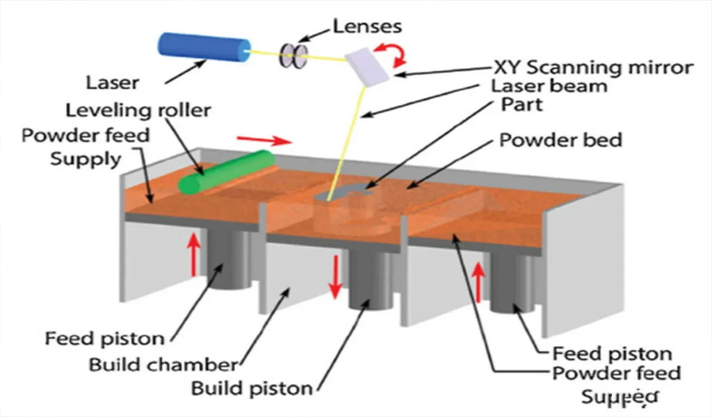
△Schematic diagram of selective laser melting (SLM) for additive manufacturing (AM)
Pure copper offers excellent physical properties, but it also has a high reflectivity to laser light in both molten and liquid states. Commercial SLM equipment typically uses lasers with wavelengths between 1000-1100 nanometers. However, within this range, pure copper has a reflectivity as high as 98%. Many scholars have pointed out the hazards of laser reflection. In a study by Jadhav et al., they exposed optical coatings without protection for 12 hours while repeatedly scanning a copper substrate with a 90% reflectivity using a laser with a wavelength of 1080nm. The figure below shows the damage to the optical coating after 12 hours of reflection. The image clearly shows significant peeling of the coating, indicating the damage caused by reflected laser light on optical components. Additionally, high reflectivity leads to energy loss, resulting in insufficient heat input.
To address the issue of inadequate heat input caused by laser reflection, researchers have employed various methods, such as using high-power single-mode fiber lasers, utilizing lasers with different wavelengths or frequencies to increase absorption, or adding other elements to the powder to enhance laser absorption.
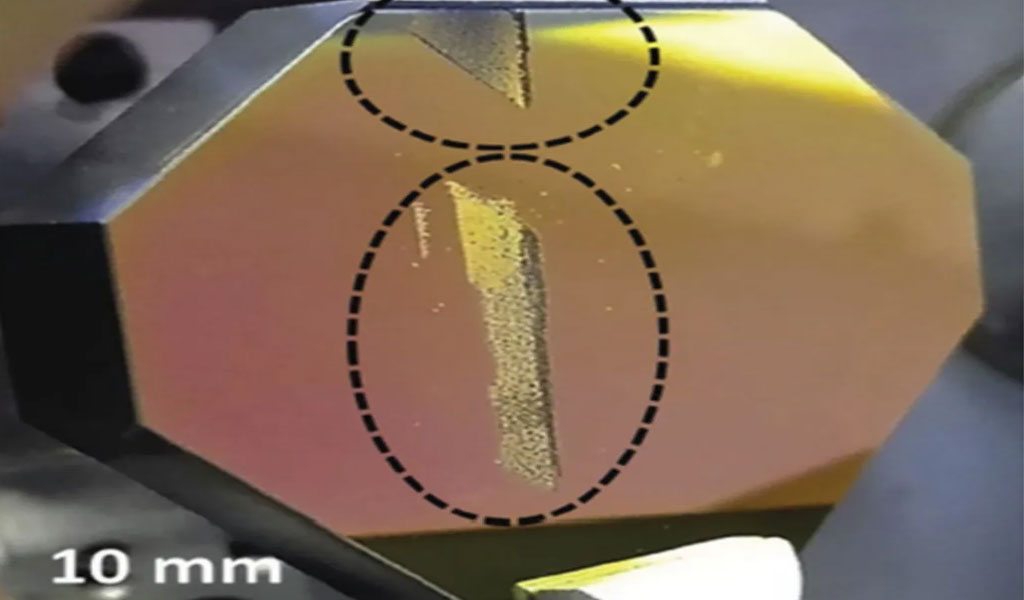
Damage to optical mirrors
Copper can absorb laser wavelengths of 515nm more easily than 1000nm. The absorption rate of metals for such laser light is as high as 25-40%. Therefore, using green lasers as the energy source for SLM 3D printing of copper can reduce the demand for laser energy and provide higher focusing accuracy. In a study by Prasad et al., to maintain the necessary heat input, they used the maximum power (1 kW) and the minimum speed (0.1 m/min) compared to additive manufacturing with aluminum, steel, and titanium. Other researchers are developing SLM technology with blue and red lasers, but studies on pure copper are still limited.
Selective Electron Beam Melting (SEBM)
Selective Electron Beam Melting (SEBM) technology is another PBF technique with principles similar to SLM technology. As shown in the figure below, SEBM technology also creates part models through 3D modeling and then produces them layer by layer through the selective melting of an electron beam. Unlike SLM technology, SEBM uses an electron beam as the heat source. The electron beam’s selective melting region is changed under the influence of electromagnetic coils.
SEBM technology has several advantages, such as a high vacuum environment that prevents oxidation of parts during manufacturing; low reflectivity, making it suitable for processing highly reflective materials; in most cases, no need for post-process heat treatment since the SEBM forming process requires preheating the substrate; and the ability to use higher power to ensure a higher processing rate.
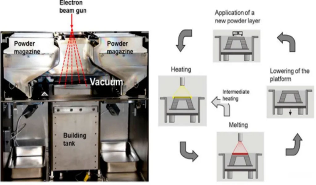
The SEBM process. Left The forming chamber. Right The 4-step process to build a layer.
Currently, SEBM technology is applied across various fields such as orthopedic implants and aerospace due to its ability to handle materials with high reflectivity differently from how they interact with electrons and photons. This makes SEBM particularly suitable for processing highly reflective materials like copper in its molten state, effectively addressing the challenge posed by copper’s high reflectivity to lasers. The technology has garnered significant attention from researchers.
Moreover, in the context of additive manufacturing with pure metals, SEBM is highly sensitive to contaminants, especially the impact of oxygen on part performance. SEBM operates under vacuum conditions, thereby mitigating the effects of oxygen in the environment. However, oxidation of pure copper powder during transportation and storage remains inevitable. Guschlbauer et al. conducted studies addressing this issue by producing parts using powders with varying oxygen content and examining its influence on part performance. They concluded that excessive oxide content can lead to cracks and other defects, severely affecting part performance.
Binder Jetting (BJ) Technology
Binder Jetting (BJ) technology originated at MIT in the 1990s. It is based on PBF techniques but differs in equipment setup. The diagram below illustrates the principle of BJ additive manufacturing technology, comprising a print head, powder spreader, heating lamp, and printing feed bed. The printing process distinguishes BJ technology from other additive manufacturing techniques: instead of using a high-energy beam to melt the powder along a planned path as in PBF, the print head sprays binder onto the powder laid on the printing bed. Subsequently, the heating lamp moves over the binder-sprayed areas for heating and curing. After the bonded part is de-powdered, it undergoes sintering and thermal debinding in a high-temperature furnace.
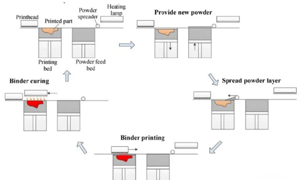
Schematic diagram of the binder jetting process steps.
With the recent advancements, Binder Jetting (BJ) technology has been widely applied to various materials including metals and ceramics. Metal additive manufacturing, in particular, has gained significant attention in current research, where BJ technology has been successfully employed with pure metals and alloys such as copper, iron, and aluminum. Due to its distinct advantages, BJ additive manufacturing has rapidly evolved:
- No Size Limitations for Parts: BJ technology allows for the production of parts without size restrictions, which is advantageous for creating large or complex geometries.
- No Need for Support Structures: Unlike traditional Powder Bed Fusion (PBF) techniques, BJ does not require support structures during the printing process, simplifying post-processing and reducing material usage.
- Wide Range of Applicable Materials: BJ can handle a broad range of materials without significant consideration for their melting points, reflectivity, or other physical properties. It can even mix different materials in a single build.
- Lower Equipment Costs: BJ systems generally have lower equipment costs compared to PBF systems, as they do not require enclosed chambers.
- Low Powder Requirements: The technology is less demanding on powder quality and does not necessarily require high-quality spherical powders, which can reduce costs.
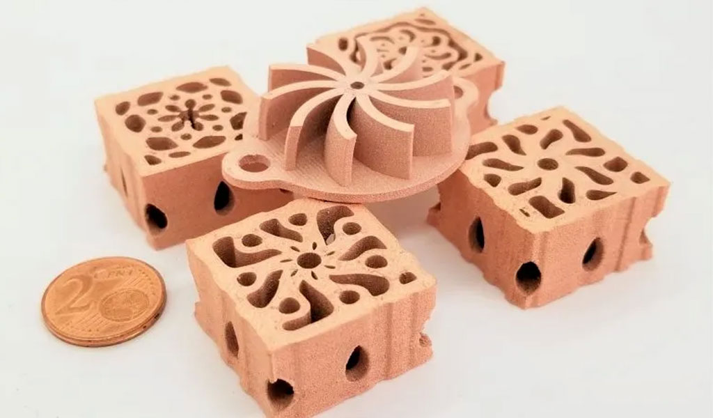
The specialized processing capabilities of BJ technology make it suitable for working with high reflectivity materials, offering a new option for additive manufacturing of pure copper components. As early as 2015, Bai et al. explored the feasibility of using BJ technology to produce pure copper components. The study discussed variations in part density, shrinkage, and tensile strength with different powder productions, ultimately achieving complex structures by adjusting process parameters as depicted in the figure below. Parts produced by BJ additive manufacturing exhibited a maximum density of 85.5%. However, the density was lower compared to parts manufactured by traditional methods, resulting in lower tensile strength due to the significant amount of binder added during the BJ process. During sintering, the decomposition of the binder leaves behind numerous pores that reduce part density and subsequently affect its performance.
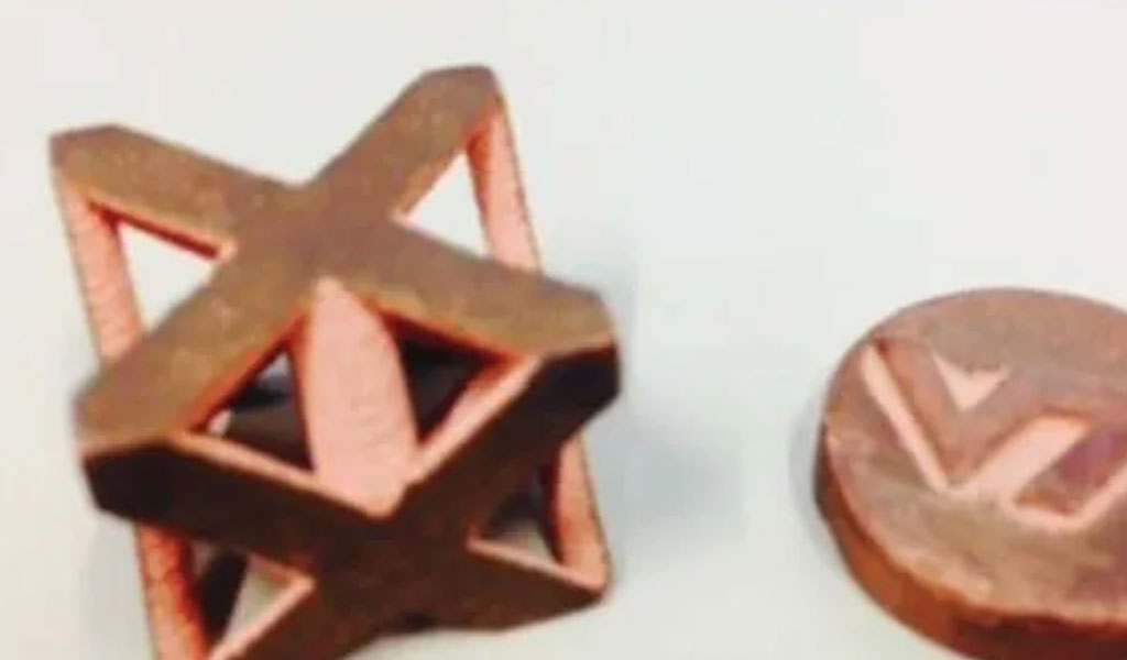
Complex copper shapes made by binder jetting
On February 27, 2021, industrial 3D printer manufacturer Digital Metal announced the launch of a new pure copper powder called DM Cu, specifically designed for Binder Jetting (BJ) 3D printing technology. This material is renowned for its excellent thermal conductivity, making it a preferred choice for heat transfer components such as heat exchangers, pipes, engines, and heat sinks for electronic products. Users can manufacture 99.9% pure copper components using Digital Metal’s DM P2500 3D printer.
According to reports, Digital Metal conducted initial experiments with the new DM Cu powder through internal testing applications. One of the applications involved 3D printing a horn antenna, which guides radio waves’ beams, showcasing the material’s suitability for high-performance applications like telecommunications and radar systems.
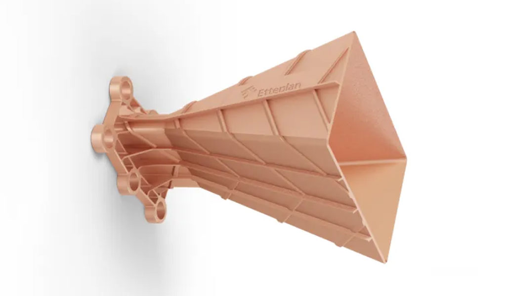
△3D printed pure copper horn antenna, picture from Digital Metal
Selective Laser Sintering (SLS)
Selective Laser Sintering (SLS) technology originated in the 1980s. Its operational principle is similar to SLM, but it utilizes materials containing a certain amount of low-melting-point polymer. Technologies like SLS and BJ, referred to as two-step methods, involve printing green parts and then achieving full density through separate operations such as post-processing or sintering. Today, SLS has become a research hotspot and is gradually being applied in industrial production. Amorim et al. studied the differences in electrical discharge machining (EDM) electrode performance between copper alloy and pure copper materials using SLS technology. This study provided a new perspective for the industry. While the final conclusion indicated suboptimal results due to significant internal porosity in parts, suggesting that EDM electrodes made from pure copper via SLS did not perform well, it nonetheless pointed directions for future research.
Ultrasonic Additive Manufacturing (UAM)
Ultrasonic Additive Manufacturing (UAM) technology differs from SLM and SEBM additive manufacturing technologies. In UAM, no external heat source is required. A small amount of heat in UAM is generated through friction. Therefore, many scholars prefer to compare UAM with processes like diffusion bonding and friction stir welding. Some researchers believe that the bonding mechanism in UAM involves a sliding action between two metal sheets. This bonding mechanism sits between diffusion bonding and friction stir welding in terms of joining mechanisms.
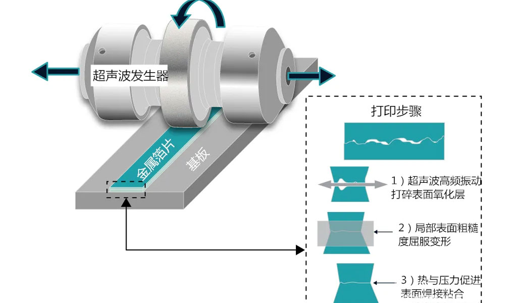
Schematic diagram of UAM technology principle
Laser Metal Deposition (LMD)
Laser Metal Deposition (LMD) is a near-net-shape Directed Energy Deposition (DED) technology. Although its forming accuracy is not as high as Powder Bed Fusion (PBF) technologies, LMD plays a significant role in the production and repair of large-scale components. Like SLM, LMD uses laser as the heat source and has gained considerable attention in recent years.
Arregui et al. studied the geometric constraints of LMD additive manufacturing of metal parts in 2018. The results showed that good forming of parts could be achieved within a range of 90-60° without adjusting the laser head. Singh et al. investigated pure copper coatings produced by LMD, with thicknesses ranging from 1-3 mm, finding that their bond strength reached 48 MPa with excellent corrosion resistance. These coatings could withstand active corrosion conditions for many years, although issues with porosity still need urgent resolution.
Yadav et al. determined the processing window of LMD through the PBF process, ultimately achieving molded parts with densities as high as 99%. The tensile properties of these parts were found to be higher than those of traditional copper parts upon testing.
LMD technology continues to evolve, offering unique advantages in the manufacture of large and complex metal components, particularly where repair and customization are essential. Its applications range from aerospace and automotive industries to tooling and rapid prototyping, reflecting its versatility and potential in modern manufacturing contexts.
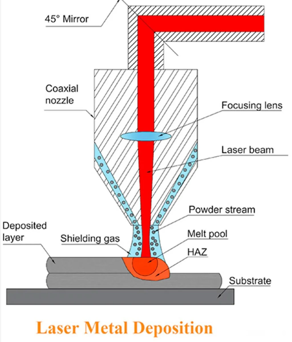
Laser Metal Deposition (LMD) Technology
Extrusion printing technology based on the FFF principle
Shenzhen Shenghua 3D, a leader in indirect 3D printing of metal ceramics in China, has developed a powder extrusion printing technology (PEP) with independent intellectual property rights. This process overcomes the challenges in the field of 3D printing and manufacturing of pure copper materials, and fills the domestic gap in pure copper 3D printing. Based on the PEP technology, 3D printing of pure copper does not require a high-energy laser beam, which cleverly avoids the problems of high thermal conductivity and high reflectivity in the pure copper printing process. Pure copper parts are obtained by first printing the green body, then degreasing and sintering. In the printing process, in order to obtain high-density or high-conductivity and high-thermal conductivity pure copper parts, the pure copper printing material formula and degreasing and sintering process requirements are also very high. Shenghua 3D pure copper granular material UPGM-CU is very suitable for pure copper 3D printing. While maintaining the high purity of the raw materials, it also has the characteristics of being easier to achieve densification, which can meet the printing needs of different copper parts. The 3D printing equipment independently developed by Sublimation 3D can process pure copper and its alloy materials to manufacture dense components, which has been widely used in the product development of heat exchangers, radiators and inductors.
German startup TSI has developed a fused filament FFF 3D printing process that can add metal or ceramic particles to the filament and ultimately obtain metal or ceramic parts, thereby providing manufacturing capabilities for space applications. As an incubated enterprise of the European Space Agency, TSI focuses on the thermal and mechanical properties of materials. Based on its high thermal conductivity, 3D printing of pure copper has always attracted much attention, and TSI hopes to launch a low-cost 3D printing solution. In June 2021, the company successfully used FFF technology to achieve high-density, complex structure, oxygen-free pure copper radiator printing.
△Pure copper heat exchanger designed by nTopology and 3D printed by TSI fused filament
Cold Spray Additive Manufacturing
Cold spray is a powder deposition method that uses the self-consolidation ability of solid powder particles to achieve mutual bonding of particles. This self-consolidation of powder can only be achieved under high-speed impact conditions. The process uses the power of kinetic energy, rather than relying on high-power lasers and expensive gases, to perform metal 3D printing at a very low cost.
SPEE3D, the supplier of metal 3D printers (special cold spray technology) and the current Australian Army manufacturing partner, has been selected by the US Navy to participate in the code-named MaintenX exercise. Through this cooperation, it is intended to promote the deployment of 3D printing in actual combat. The biggest advantage of SPEE3D’s process is the low cost and shortened time of 3D printing. For example, the copper wheel shown in the figure below was completed in only 2.8 minutes and cost only $10, which is a huge price advantage.
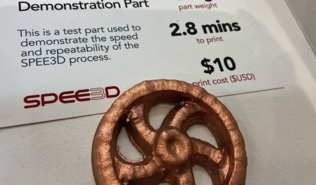
SPEE3D prints copper wheels in just 2.8 minutes
Photocuring technology
In August 2021, Holo, a US company, launched a technology called PureForm, which uses photopolymer slurry and stereolithography (SLA) to manufacture precision metal parts. It is still rare in China. The specific working principle of this technology is:
- ① Prepare a proprietary metal-polymer slurry;
- ② Print with a photocuring 3D printer;
- ③ Obtain a dense metal particle polymer matrix;
- ④ Degreasing;
- ⑤ Sintering to obtain a fully dense part
Because it is printed using photocuring technology, the accuracy is relatively high and a structure of 150-200 microns can be produced. Holo’s slurry has excellent dispersibility and can form a uniform layer thickness during the printing process. The printer can cure the new layer in less than 10 seconds. At present, the density of pure copper formed by Holo through the DLP+ degreasing and sintering process is an average of 96-98%, which is enough to achieve 95% of the thermal conductivity and electrical conductivity of bulk copper. In addition, this process may also reduce the cracking problem caused by laser printing.
Prospects and challenges of 3D printing copper
Copper and copper alloys are widely used in electricity, heat dissipation, pipelines, decoration and other fields due to their excellent electrical conductivity, thermal conductivity, corrosion resistance and toughness. Some copper alloy materials have good electrical conductivity, thermal conductivity and relatively high strength. They are widely used to manufacture combustion chamber components of electronic, aviation and aerospace engines. Today, we are facing the challenges of industrial lightweighting and structural complexity. Additive manufacturing technology can solve these problems well.
In order to ensure the performance and availability of parts in actual production, a suitable additive manufacturing method should be selected. The parts produced by SLM have high precision, but the reflectivity of copper is high, and the adaptability of process parameters is high. In addition, due to the rapid heating and rapid cooling of the SLM processing method, large internal stress is easily generated inside the sample. Although the influence of internal stress can be reduced by matrix preheating and post-treatment, it also increases the complexity of the process [97]. SEBM technology is a method more suitable for pure copper additives, but at the same time, due to the high price of equipment, the widespread application of this technology is limited, and the precision of the parts produced is also slightly lower than that of SLM technology [93]. BJ technology can produce green parts at low energy density, and it must be reprocessed. Compared with SLM and SEBM technologies, BJ technology is difficult to ensure the accuracy of parts during post-processing, and the parameters during sintering also have a great influence on the forming of parts.
In addition, pure copper has antibacterial and catalytic effects in addition to good electrical and thermal conductivity. In the study of Wang et al., an alternating deposited nickel-copper coating was produced, which has both good wear resistance and antibacterial properties. This provides new ideas and directions for the application of pure copper, which can be combined with other metals to produce complex medical tools. At the same time, in the study of Yang et al., they found that CuO can catalyze the decomposition of azo compounds, and the use of nanoporous structures not only increases the specific surface area, but also avoids the waste of raw materials, so that the catalyst can be recycled.
Antarctic Bear believes that the potential of additive manufacturing has not been fully explored, and researchers still have a heavy task. At present, people are just beginning to understand the process of additive manufacturing and recognize its potential. In future development, better process control is needed to further improve the forming and performance of parts. Different processing methods have different advantages, and the unremitting efforts of researchers will eventually promote the progress of pure copper parts production. Driven by these technologies, it is expected that solutions will be found to the processing problems of pure copper parts, accelerating the development and progress of various industries.