Researchers use inkjet technology to 3D print graphene to produce electronic devices
Graphene composed of single carbon atoms is considered to be a high-quality material with a wide range of applications due to its high strength, light weight, flexibility and unprecedented conductivity. However, mass production of large graphene parts remains a challenge. Previous research has shown that there are various methods for 3D printing graphene, but the size of these technologies is still limited. In addition, these methods and non-additive methods for producing large-area graphene layers hinder certain desirable properties of the material, namely, electrical conductivity.
Now, researchers at the University of Nottingham have developed a technology for 3D printing graphene using inkjet technology, which can maintain the electrical properties of the material, thereby opening up possibilities for a series of electronic components such as transistors and sensors . The research titled “Quantum Transport of Electrons and Holes between Sheets in Inkjet Printed Graphene Devices” was published in the journal Advanced Functional Materials.
A 3D-printed phototransistor, which consists of “exfoliated InSe flakes and six inkjet printed graphene strips (each electrode contains 5 printed layers, 7 lines) on a 300 nm SiO2/Si substrate in contact with each other. These strips are used as electrodes.”
As a two-dimensional material, graphene is usually made by peeling off the various layers of carob atoms in the form of a flat plate. Then, to process multilayer objects of this material, these plates need to be deposited manually, which is obviously a laborious process. In order to make full use of the characteristics of this exotic material through a scalable process, the Nottingham University team developed an inkjet method that can inkjet ink containing graphene flakes. In addition, by using quantum mechanical modeling, researchers can accurately understand how electrons move through the graphene layer, thereby controlling the electrical properties of the printed material.
Professor Mark Fromhold, Dean of the School of Physics and Astronomy and co-author of the paper, said: “By linking the basic concepts in quantum physics with the latest technology, we have shown how to pass printing thickness Only a few atoms but a few centimeters wide layers of materials are used to make complex devices for controlling electricity and light. According to the laws of quantum mechanics, where electrons act as waves instead of particles, we find that electrons in two-dimensional materials travel along multiple sheets. The electrons seem to jump from one slice to another, like a frog jumping between overlapping water lilies on the surface of a pond.”
In order to print the material, a graphene ink composed of graphene flakes and ethyl cellulose was dispersed in a cyclohexanone/terpineol mixture, and it was printed on a substrate using a drop-on-demand printing method. The layers were then annealed in a vacuum oven at 250°C to remove the solvent and decompose the additives in the ink. The research team found that the larger the number of layers, the lower the resistance. To demonstrate the possibility of this material, the team 3D printed a phototransistor composed of graphene electrodes on a semiconductor crystal.
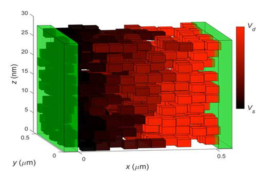
The key to this research is to understand the movement of electrons in order to best produce graphene parts. To this end, the team modeled the conductive properties of the flake network within the printed part, and simulated the charge transfer between graphene flakes when a virtual voltage was applied to the simulation device. The author points out: “Our model reveals the transport mechanism of carriers in the printed graphene layer and shows that to obtain a high-conductivity device, an optimized thickness of the printed layer with high [fill rate] is required.”
In order to understand how printed graphene works in devices made of multiple materials, the researchers printed field-effect transistors in 3D. Due to the interlayer ink mixing, the resistance is actually higher than the resistance of five graphene printed layers.
Optical microscope image of 3D printed graphene field effect transistor; “The scale bar is 500 µm, and the spacing between the silver electrodes is 100 µm.”
Comment: Although the 2D layers and equipment were previously 3D printed, this is the first time anyone has determined how electrons move through them, and proves the potential use of the combined printed layer. The results of this research may lead to various applications of inkjet-printed graphene-polymer composites and a series of other 2D materials. This discovery can be used to manufacture a new generation of functional optoelectronic devices. For example, large and efficient solar cells; wearable flexible electronic devices powered by sunlight or the wearer’s movement; and even printed computers. “
Next, the team plans to improve the deposition of graphene by using polymers to affect the way the flakes are arranged. They also hope to use different types of inks with graphene flakes of different sizes. The researchers will also improve their computer simulations to include how different materials work together. Ultimately, they aim to develop methods for mass production of prototype devices.