The development of electronic devices and hardware is generally a time-consuming process. Compared with software development, electronic R&D tends to require more upfront investment and face economic risks, and this economic risk is likely to increase throughout the project cycle. The cost of making some changes in a new product involves a wide range, and these costs will often increase as the development process progresses. The goal of the industrial field is always to make the new design perfect in the prototype stage.
In response to these risks in hardware R&D, more and more design teams are adopting flexible hardware R&D processes to develop new electronic products. These flexible product development processes are being integrated into the design process, because these methods are making it easier for the design team to adapt to product changes or customer needs. Since prototypes, testing, and redesign based on test results are the basic parts of hardware design, it is very important to understand the role of each link in prototyping.
Flexible hardware R&D adapting to flexible software practices can reduce R&D costs and time
Prototype design is very important for the effectiveness of different design results testing, and redesigned optimized variables and more complex products require a series of simulations and experiments to test their functionality. Simulation and testing feedback to product changes and multiple redesigns in the design process represent an iterative system at the core of flexible hardware development. The use of 3D printing for PCB prototype design can enable the hardware development process to be truly iterated while reducing or eliminating economic risks.
It can help deal with risks in hardware R&D
Due to the investment and economic risks involved in the research and development of electronic devices, electronic designers have become risk aversions, which will hinder innovation and cause engineers and product designers to become very conservative in design concepts. Because of the many complex products, they tend to rely on heavy simulation analysis to design their experience products, and the test results are only obtained through a small number of prototype tests. Due to the cost and time involved in the prototype stage, and the cost of redesign, it is difficult for a design team to bear any errors and time for correction.
As a result, designers have become very reluctant to build complex and innovative products. They are imprisoned in traditional linear R&D design to adapt to traditional PCB production. The traditional PCB production process sets too many constraints in terms of design freedom, limiting the number of tests and redesigns that cannot exceed the budgeted cost. These stifle the designer’s innovation in using upgraded devices in new products.
More and more complex products require repeated iterations of design, model building and testing during the product development phase. These design, build, and test iterations are at the core of flexible software and hardware development. Each iteration allows a product development team to confirm and adapt to important design changes in the early design process. Any PCB designer knows that early confirmation of these changes in requirements can additionally reduce the scope of product redesign, which can reduce the overall development time and cost.
A product design team must be able to adapt to the overall changes in the development process. The design, testing, and construction iterations in the hardware development process can make these changes confirmed and executed before the final product design. The models built before the design requirements change are all floating on the surface, because customer requirements change at any time, device defects, and simulation results. Similarly, some design changes in requirements will only become significant after the final prototype is tested.
Using the 3D printing system to make prototype parts allows you to test the functionality of the principle prototype in different iterations, while the processing cost and delivery time are determined. When your design team has obtained a PCB 3D printing system, you can use a fixed time to create a single sample of a complex PCB board at multiple points in the PCB design process. This allows the design team to frequently check the functionality of the design in the early design stage at the lowest cost. In general, the speed of the research and development cycle has brought designers a lot of freedom in the design of the interactive connection structure of the PCB board, the embedding of the device and the geometry of the substrate.
Flexible hardware development process design, model construction and testing
When you can make prototypes with a fixed cost structure and delivery time, you can reduce many of the risks involved in producing prototypes with traditional processes. One of the benefits is that prototypes can be tested quickly. This can quickly allow the design team to get design feedback to improve functionality and meet customer needs. Since the production time of 3D printing is not related to the complexity of the device, you can quickly repeat production and test prototypes during the design sprint.
As a hardware development link, use a 3D printing system to print these boards or more complex products within a few hours
During the rapid development of each product, a flexible hardware R&D team can determine the appropriate time to produce and test prototypes to evaluate design functionality. 3D printing allows you to manufacture complex devices, such as manufacturing PCB boards in a few hours instead of days. The proposed design changes can be quickly evaluated through testing. This method can confirm the correctness of the simulation analysis results, and can help the embedded system designer confirm and modify software bugs.
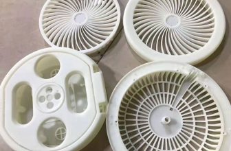
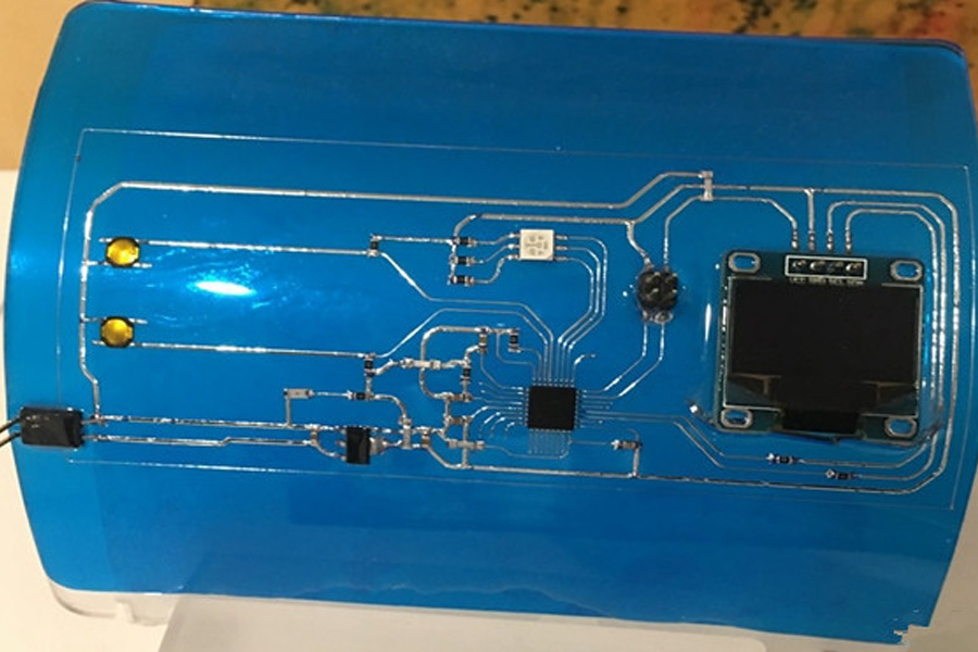
Flexible hardware development process design, model construction and test iterations, the application of 3D printing system is not only limited to printing PCB boards. Special structure and functional devices, such as printed antennas, embedded devices, non-orthogonal inter-layer interconnections, and non-planar substrates, can all be iteratively tested and optimized during the design stage. This flexible hardware development workflow provides design teams with a cost-effective way to innovate and improve product quality.
Additive technology optimizes prototyping
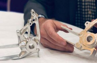
If you are considering the production of new full-size products using a 3D printing system, it makes sense to use a 3D printing system to manufacture hand-made models. Your prototype will be very similar to the final product, which will give you a more intuitive understanding of the design factors that affect the function of the PCB board. Similarly, you can ensure that your design is manufactured in full scale, ultimately increasing output. Prototyping is an indispensable part of flexible hardware development. The application of a 3D printing system allows you to produce prototypes at a fixed cost, predictable delivery time and basically the same as the final product.
The editor believes that the advantages of additive manufacturing of electronic products will be integrated into the early stages of product design and development like metal and plastic printing methods currently on the market. PCB3D printing needs to consider the connection with traditional manufacturing in the manufacturing process. It is necessary to find plates that are difficult to solve by traditional manufacturing or difficult to process. In the future, it may be more inclined to develop innovative functional components, such as 3D antennas, 3D-MID, and 3D. Electronic interconnection structure and so on. The application of these devices needs to try to adopt new design methods for verification, and it is hoped that the official will release some guiding design principles in specific areas.